Longi shows how edge masking raises lab solar efficiency readings
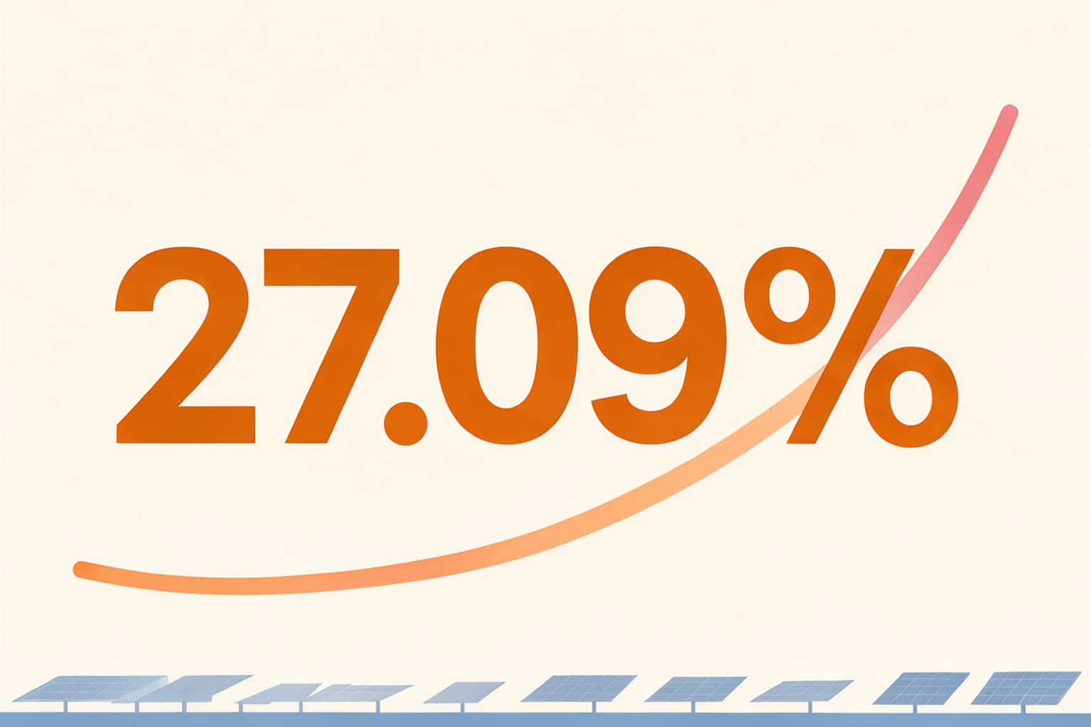
Cover the edge of a solar cell with an opaque material during testing and its measured efficiency goes up. Longi researcher Genshun Wang and his colleagues wanted to understand why. The question came from an earlier study on high-efficiency back-contact cells, where the team found that the wafer edge was a major channel of current loss, and that masking it raised the measured efficiency to 27.09% over the designated illumination area, against 26.74% over the total area.
Charge carriers, the electrons and holes that light releases in silicon, are lost when they recombine before reaching the contacts. Wang said earlier work had treated the masked strip as simple geometric shielding, or as a parallel dark sink in a circuit model, with little said about how carriers actually move. Using Quokka 3 simulations, the team showed that the mask turns the outer region from an illuminated, conductive area into a dark, resistive one. This “resistive barrier” keeps carriers from drifting toward the edge, which is where they would otherwise recombine and be lost.
The experiments located an optimum. A 5 mm mask gave the best result, while masks of 10 mm and 15 mm reduced efficiency because the inactive area grew and brought its own electrical losses. Short-circuit current density first rose with mask width, while open-circuit voltage fell. In cells without edge passivation, the gain was about 0.2 percentage points. The simulations also showed that carriers can still reach the masked region through the metal grid lines, which limits the benefit. The team proposed removing metallization from the masked area to isolate the edge electrically, and its model predicts gains in fill factor and open-circuit voltage from that change.
What changes is mainly for the people who measure cells. Labs that publish efficiency records can separate edge losses from the other factors that limit a device, and cell designers can calculate the mask width that gives the largest masking gain, so that a suitable grid layout can deliver it. The paper, published in Solar Energy Materials and Solar Cells, gives no timeline, and the authors are clear about the limit: “It is worth stressing that this is not a production technology,” Wang said. Selective metallization adds process complexity, and the masked area generates no power, so it lowers the share of total cell area that produces electricity.
Comments
Loading the thread…
Sign in to leave a comment. Sign in